Microprocessor, the core of the contemporary electronics industry. Whether it is smart watches, smart phones, smart appliances and other consumer electronics products, supercomputers, automotive engine control, CNC machine tools, precision guided missile technology are sophisticated products are inseparable from the role of the microprocessor. Microprocessors, generally composed of one or a few large-scale integrated circuits, can read and execute instructions and exchange data with external memory and logic components, and is the core computing control part of microcomputers. Today, the material used in microprocessor manufacturing is essentially silicon. The bottleneck of silicon materials such as the following two main aspects: First, performance bottlenecks, and now silicon semiconductor chips, slowing performance growth, and close to the physical limits. The second is not flexible, silicon materials can not be used in the field of flexible electronics. A two-dimensional material refers to a material in which electrons can move freely (planar motion) only on non-nanoscale (1-100 nm) in two dimensions such as graphene, boron nitride, transition metal compounds (molybdenum disulfide, disulfide Tungsten, tungsten diselenide), black phosphorus and the like. Two-dimensional materials, usually composed of one or several layers of atoms, the focus of our previous graphene is a well-known two-dimensional material. In addition, graphene-like materials such as transition metal dichalcogenides also belong to two-dimensional materials. They are not only small in size, thin and soft, but most importantly they have excellent semiconductor properties and are very suitable for flexible electronic devices . Dr. Thomas Mueller, Ph.D. Institute of Photonics, Vienna University of Technology, has been working on two-dimensional materials research, he said two-dimensional material is the future of microprocessors and other integrated circuits ideal candidate material. The molybdenum disulfide (MoS2), composed of molybdenum atoms and sulfur atoms, the thickness of only three atoms, is such a two-dimensional material. So he led the research team at the Technical University of Vienna in collaboration with scientists at the flagship EU graphene project to create a transistor made of two-dimensional MoS2 molybdenum disulfide material. 115 such transistors constitute a new type of microprocessor. At present, this kind of microprocessor can carry out one-bit logic operation, and the future is expected to expand to multi-bit operation. The thinness of MoS2 means that transistors have high responsivity. Mueller said: "In principle, it is advantageous to provide a thin material for the transistor, the thinner the transistor, the better the static control of the transistor channel and the lower the power consumption. So far, the MoS2 microprocessor is one of the most advanced circuits made of two-dimensional materials. Test run simple program shows that the microprocessor has excellent signal quality, and lower power consumption, and get the correct operation results. This ultra-thin MoS2 transistor is small in size and flexible enough to be fabricated into flexible electronic devices such as wearable devices and smart hardware, which are widely used in the Internet of Things. In this regard, Dr. Thomas Mueller said: "In general, becoming a soft material will lead to new applications, one of which may be the combination of these processor circuits and a light emitter made of MoS2 to create a flexible Display devices and electronic paper, or integrate them into the logic of smart sensors. " Modern microprocessors, typically made of silicon, have millions of transistors on a single chip, so it's easy to say that a device made of MoS2 with only 115 transistors. However, Dr. Stefan Wachter, Ph.D. student in Dr. Mueller's group, said: "Although this is a glaring contrast to the current silicon-based industry standards, it is an important breakthrough in this area of ​​research. Now that we have With proof of concept, in principle there is no reason not to see future progress. " This chip just shows the early results of this new technology, we can believe it will have greater results in the future. For the team's next plan, Mueller explained: "Our goal is to achieve larger circuits that can do more with useful operations and we want to complete a full eight bits on a single smaller chip Design, or more bits. "But because of this design and manufacturing, this goal will be challenged, so Stefan Wachter said:" Adding more bits, of course, will make everything more complicated, for example, adding only one Bit, it will double the complexity of the circuit. " Future outlook: Two-dimensional materials such as molybdenum disulfide, though promising to be a substitute for silicon. However, these circuits require thousands or even millions of transistors to make more complex circuits, and for the time being can not rely on this new technology. After all, the process of producing 2D materials and further processing 2D materials is still in its infancy. So, at present, it is just a complementary technology for silicon semiconductor technology. In response, Dr. Mueller explains: "Our circuits are more or less hand-made in the lab, and it's clearly beyond our ability to design complex circuits. Each transistor must be programmed to work on The unit can work as a unit. "In addition, future enhancements to multi-stage design processes will be an important step toward developing high-volume production solutions for MoS2 microprocessors. Because in all factors, transmitting large areas, double MoS2 to the wafer, will bring a high failure rate. Therefore, Dmitry Polyushkin of the Technical University of Vienna said: "Our solution is to raise the process to a point where we can reliably produce chips with tens of thousands of transistors, for example directly on a chip, which will avoid the transfer process. This leads to higher yields, allowing us to produce more complex circuits. " Researchers believe there will be a wide variety of new industrial applications for this technology in the coming years, as is the case with flexible electronics, such as medical sensors and flexible displays. Because 2D materials have more mechanical flexibility than traditional silicon materials.
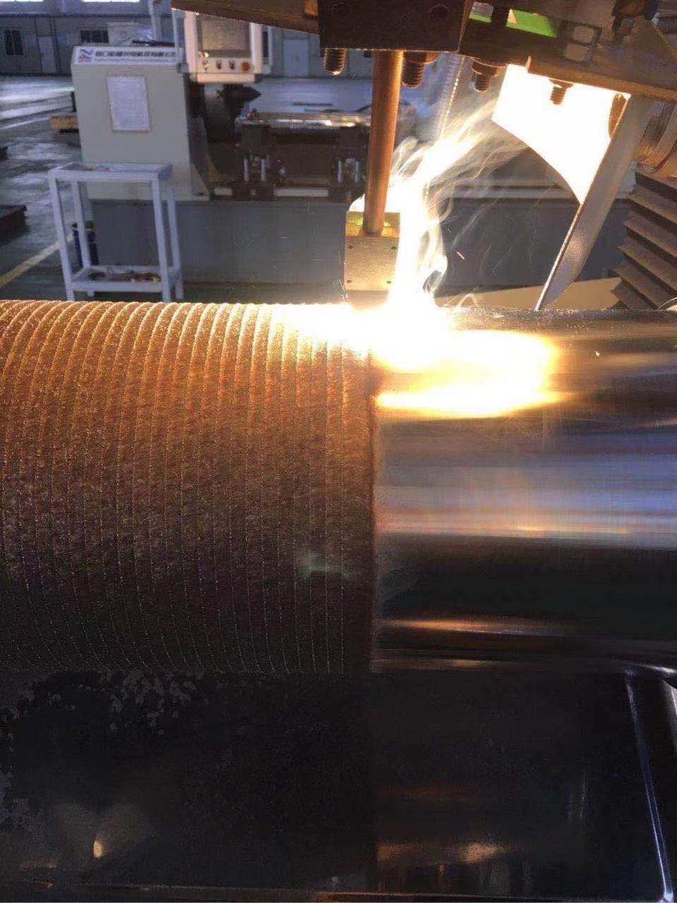
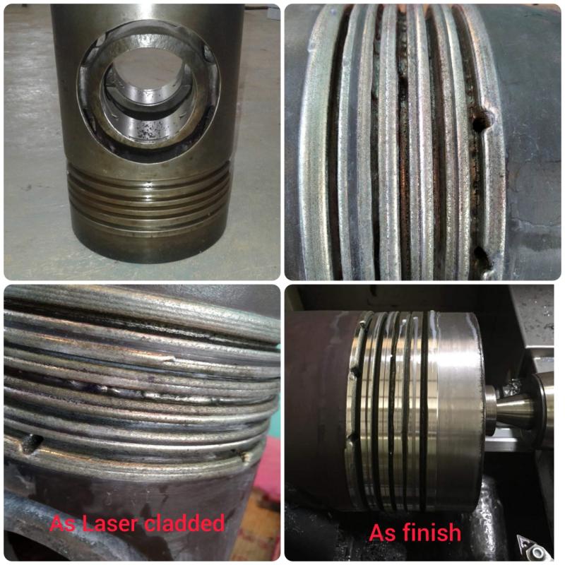
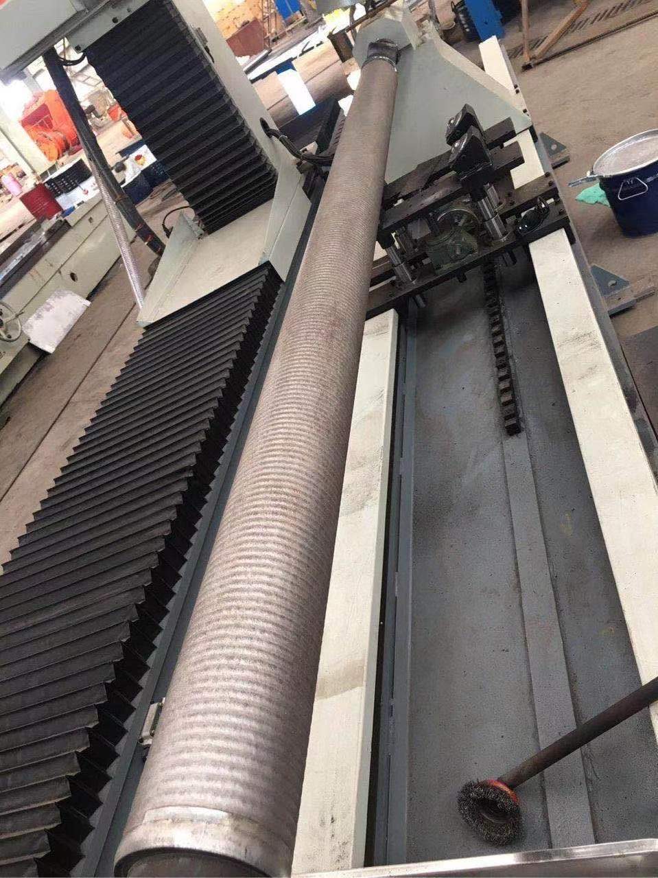
Nickel Based Laser
Cladding Powder
Ni base alloy
powder is mainly made of NiCrBSi or NiBSi. Ni-based self-fluxing powder has
good wettability, corrosion resistance and high temperature self-lubricating
effect, and is used in components with heat resistance, corrosion resistance and
thermal fatigue resistance. In general Ni35,Ni45,Ni60 etc can be used for laser
cladding, the No means hardness of powder. Inconel 625 and 718 has good
corrosion property under higher temperature, also widely used for laser
cladding process.
Cobalt based Laser
Cladding Powder
Cobalt-based alloy
powder is the cemented carbide resistant to various types of wear and corrosion
as well as high temperature oxidation. That is, the so-called
cobalt-chromium-tungsten (molybdenum) alloy or Stellite alloy cobalt-based
alloy is mainly composed of cobalt, containing a considerable amount of nickel,
chromium, tungsten and a small amount of molybdenum, niobium, tantalum,
titanium, Alloying elements such as lanthanum, and occasionally a class of
alloys containing iron.
Co-based self-fluxing
alloys have good high temperature performance and wear resistance and corrosion
resistance, and are used in petrochemical power, metallurgy and other
industrial fields where they are wear-resistant, corrosion-resistant and
high-temperature resistant.
Iron based Laser
Cladding Powder
The work pieces
required for laser cladding and manufacturing in the actual industry are mainly
carbon steel and cast steel. The Fe-based alloy is close to the base material
in composition and has good wettability. The advantage of Fe base powder is
lower cost and good wear resistant of cladding layer. As a result, it`s the
most widely used for laser cladding process. It is suitable for parts that
require local wear resistance and are easily deformed.
WC blended Laser
Cladding Powder
Tungsten carbide blended with Ni alloy powder is the best
choice for wear resistant work piece. This unique process can bring excellent
wear, corrosion and high temperature resistant. Our blend powder can achieve
different portion of WC from 35% to 60% without crack under suitable cladding
parameter.
Iron Alloy Powder,Nickel Alloy Powder,Cobalt Alloy Powder,Laser Cladding Powder Luoyang Golden Egret Geotools Co., Ltd , https://www.xtcalloypowder.com


